
Custom Layout Design
Custom & Compiler Memory Layout

End-to-End Solutions for memory layout services from design and development
through tapeout and signoff, including seamless IP migration across technology nodes
and foundries
SRAM: Single-Port, Dual-Port, and advanced SRAM variants
ROM: Single-Port, Dual-Port, and customized ROM architectures
Register Files (RF): High-performance and high-density memory architectures
Flash Memory: Custom Flash memory layout and integration support
DRAM: High-density DRAM layout and technology-specific implementation
Technology Migration: Porting and optimisation across different process nodes and
foundries
Tapeout & Signoff: Full physical verification, reliability checks, and tapeout-ready
delivery
Analog & Mixed-Signal Design Expertise

High-Speed Connectivity: SERDES, HSIO, and DDR interfaces
Clocking & Timing: Digital PLLs, Low-Jitter Ring PLLs, and LC PLLs
Data Converter Solutions: Pipeline & SAR ADCs, and Current-Steering DACs
Power Management: LDOs, DC-DC Converters, and Power Management IPs
Precision References: Bandgap Reference and bias-generation circuits
RF & Frequency Synthesis: RF Synthesizers, Mixers, LO Generation & Distribution
RF Front-End: Low-Noise Amplifiers (LNA) and Power Amplifiers (PA)
Custom Full-Chip Layout & Integration
IO Ring Architecture & Automation – Robust IO ring planning, generation, and layout automation.
Package & Pad Integration – Support for Flip-Chip, Wire-Bond, and advanced pad configurations.
Full-Chip ESD Strategy – ESD-aware planning, protection strategy, and implementation across the complete chip.
Analog & Digital Integration – Seamless integration of Analog IPs, Custom Blocks, and Digital Macros.
Physical Verification & Signoff – Comprehensive DRC, LVS, ERC, antenna, and full-chip physical verification.
Power Planning & Integrity – Power-grid design, EM/IR analysis, voltage-drop optimization, and reliability signoff.
Full-Chip Layout Assembly – Hierarchical integration, floorplanning, block alignment, routing coordination, and tapeout-ready layout delivery.
Foundation IP & Library Solutions
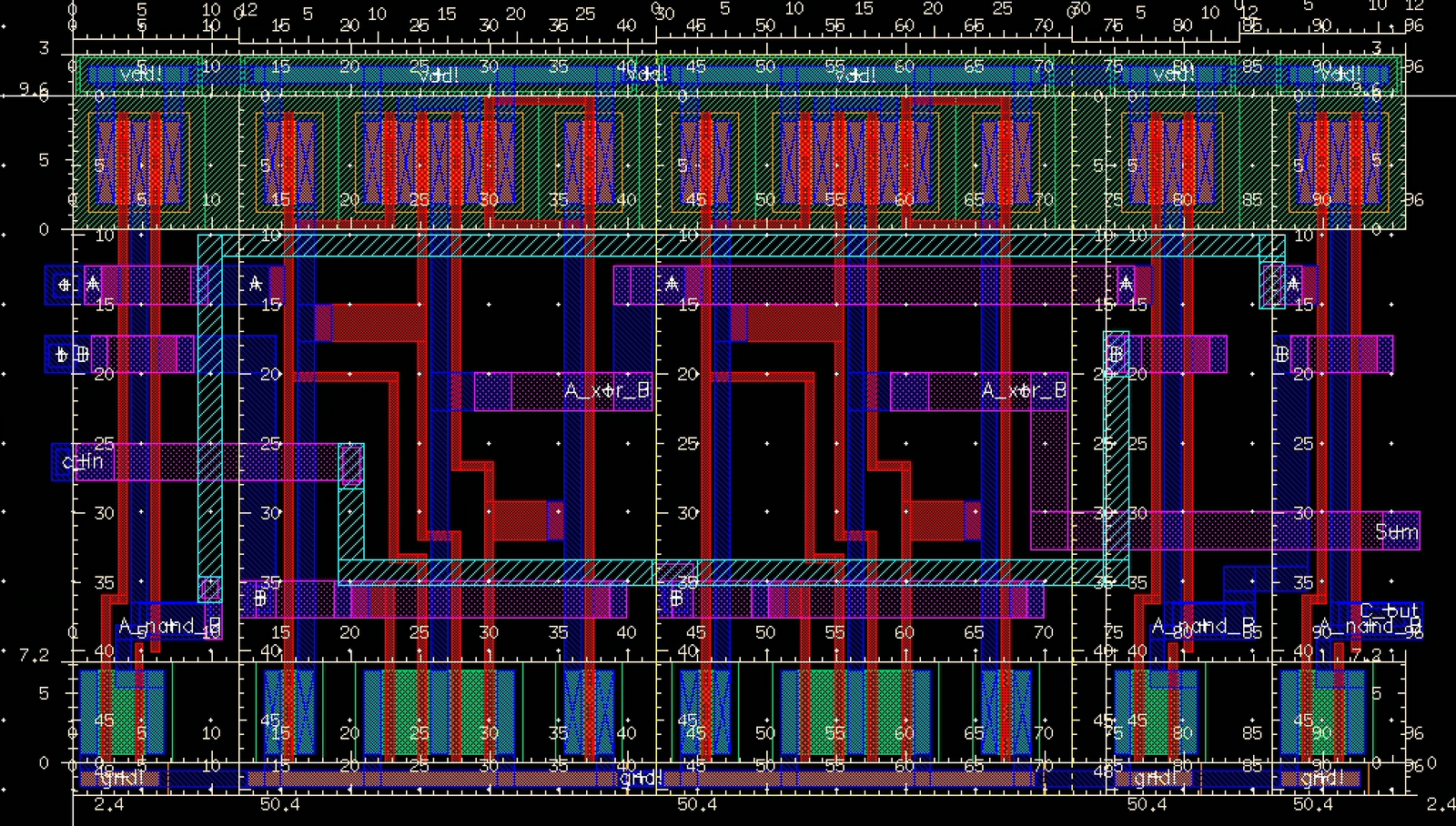
Standard Cell,& I/O Libraries — End-to-end development of high-performance, high-density, and
application-specific libraries.
Layout & Model Generation — Complete physical layout, characterization, and model generation for
production-ready IP libraries.
Layout Architecture & Strategy — Definition of optimized layout architectures and methodologies
addressing EM, lithography, OPC, density, and manufacturability requirements.
DFM-Optimized & High-Density Libraries — Development of DFM-compliant, ultra-high-density, and performance-optimized library solutions for advanced technology nodes.
Physical Design Services
Physical design

Full-Chip Physical Design Services
Synthesis – Logical and physical-aware synthesis
DFT – Advanced scan insertion for robust testability.
Floorplanning – Hierarchical and flat partitioning for efficient chip architecture.
Place & Route – High-performance placement and routing for complex designs.
Clock Tree Synthesis – Balanced, low-skew clock distribution.
Power & EMIR Analysis – Comprehensive power integrity and reliability checks.
Low-Power & LEC – Verification of low-power intent and logical equivalence.
Functional ECOs – Fast and reliable engineering change implementations.
Physical Verification & Signoff – Complete verification for tapeout-ready silicon.
IP Hardening – DDR, MPHY, DPHY, and eMMC PHY integration with proven reliability.
Full-Chip Delivery – End-to-end physical design for signoff-ready silicon.
Full Chip Physical design

Top-Level & IO Planning
Bump Planning & Analysis – Optimised bump design for signal and
power integrity.
RDL Routing – Reliable redistribution layer routing from bump to IO
pad (signal/power).
Power Planning – Robust chip-level power distribution strategy.
3rd-Party IP Integration – Seamless integration of external IPs into
top-level design.
IO Pad Placement & Analysis – Signal- and power-aware IO pad
optimization.
IO & Seal Ring Creation – Complete IO ring and seal ring
implementation.
Special Net Routing – Manual routing for sensitive analog and clock
nets.
Core Protection Placement – ESD, TCD, ICOVL, BEOL/FEOL
structures for reliability.
Packaging Collaboration – Close interaction with packaging teams
for end-to-end delivery.
STA
Timing & Signoff Services
SDC Development – Robust constraint creation for accurate
timing analysis.
Top-Level Timing Budgeting – Precise chip-level timing
allocation and management.
SI-Aware Analysis – Noise library–based signal integrity
timing checks.
MMMC Validation – Multi-mode, multi-corner setup and
validation.
Timing Closure – Functional and test-mode closure for
reliable silicon.
Advanced OCV Derates – ΔV and ΔT–based special derate
assessments.
Timing ECOs – Fast implementation for functional, shift,
capture, and BIST modes.